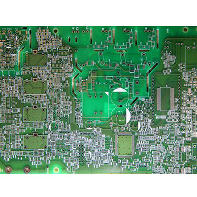
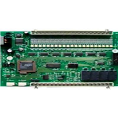
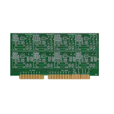
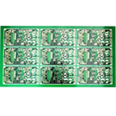
Product Profile of Multi-Layered Printed Circuit Board
Multi-Layered Printed Circuit Board features finished hole of minimum 0.3mm size range. The Printed Circuit Board is offered in a thickness range of 0.8 to 3.2mm with finished copper of 3 oz for outer layers and 2 oz for inner layers. The Printed Circuit Board is made using quality grade raw material. Multi-Layered Printed Circuit Board can be availed in different surface finishes to suit industrial requirement.
Key Features of Multi-Layered Printed Circuit Board
- Features finished hole of minimum 0.3mm size range
- Offered in a thickness range of 0.8 to 3.2mm with finished copper of 3 oz for outer layers and 2 oz for inner layers
- Made using quality grade raw material
- Surface Finish: HASL / HAL LEAD FREE / ENIG / OSP