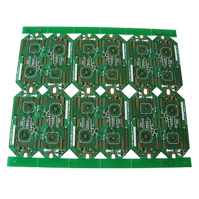
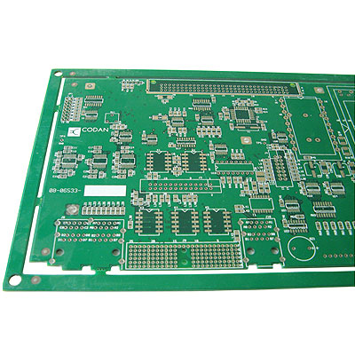
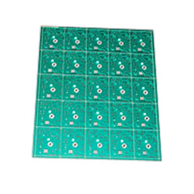
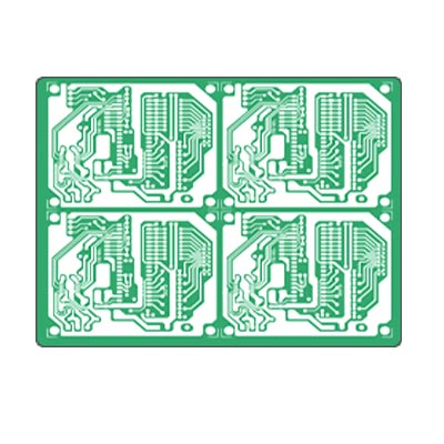
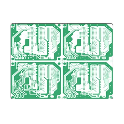
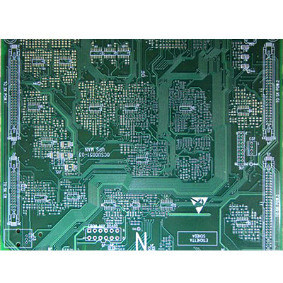
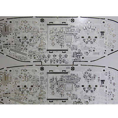
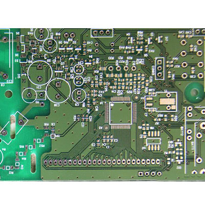
Product Profile of Double Layer Printed Circuit Board
Double Layer Printed Circuit Board is available in a thickness range of 0.8 to 3.2mm.
The Printed Circuit Board is offered in line width and spacing of 6 / 6 mils. The Printed Circuit Board is featured with minimum finished hole of 0.3mm size range. Printed Circuit Board finds application in automotive, energy, peripherals and industrial automation sectors. Double Layer Printed Circuit Board is offered with surface finish of solder levelling, lead free hot air levelling, chemical tin or chemical gold.
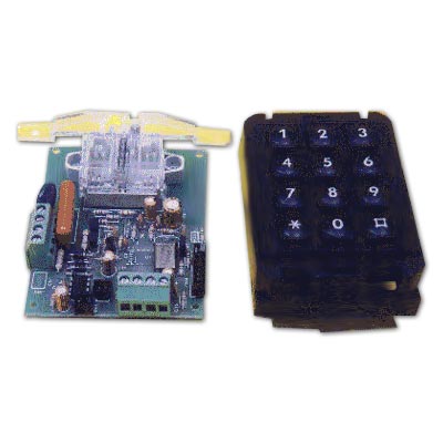
Applications of Double Layer Printed Circuit Board:
Automotive
Energy
Peripherals
Industrial Automation sectors
Key specifications of Double Layer Printed Circuit Board:
Thickness of 0.8 to 3.2mm [with finish copper of 3 oz]
Line width and spacing of 6 / 6 mils [sample lots 5/5mils]
Minimum finished hole size of 0.3mm
Surface finish of solder levelling, lead free hot air levelling, chemical tin or chemical gold